


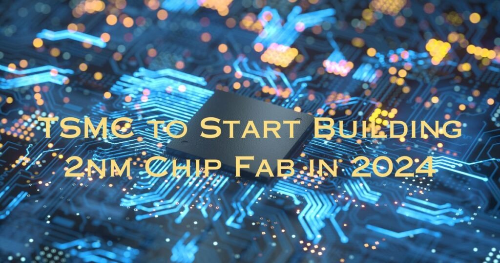
TSMC’s Leap into the Future: Building a 2nm Chip Fab in 2024 with Gate-All-Around Transistors
In the fast-paced world of semiconductors, Taiwan Semiconductor Manufacturing Co. (TSMC) is gearing up for a groundbreaking move. The semiconductor giant is slated to commence the installation of equipment into its 2nm-capable fabrication plant in the Hsinchu Science Park come April 2024. This strategic move signifies a substantial leap forward for the TSMC N2 project.
The Powerhouse of Innovation
As the world’s leading contract chipmaker, TSMC has played a pivotal role in supplying chips to tech giants like Apple, Nvidia, AMD, Qualcomm, and more. TSMC’s success over the last two decades stems from its consistent ability to introduce new manufacturing technologies with notable power, performance, and area (PPA) enhancements annually. The company has been introducing a fresh node every 18 to 24 months while maintaining impressively high yields.
However, with the complexity of modern fabrication processes reaching unprecedented levels, sustaining this pace of innovation alongside predictable yields and simple design principles is becoming increasingly challenging.
The 2nm Race: TSMC vs. Samsung
In the race for 2nm supremacy, TSMC finds itself in a head-to-head competition with Samsung. Both companies are developing their versions of gate-all-around (GAA) technology. Samsung, in particular, is working on its multi-bridge channel field-effect transistor (MBCFET). The stakes are high, with TSMC asserting that its N2 technology will be the most advanced in both density and energy efficiency when it hits volume production in 2025.
While TSMC remains confident in the progress of its N2 technology, the industry awaits to see if Samsung can present a challenge with superior yield and production capacity.
Blueprint for the Future
TSMC’s plan involves constructing a 2nm chip fab in Hsinchu, a significant chip manufacturing center in Taiwan. The company received approval from the country’s Environmental Review Committee to initiate construction in early 2022. The subsequent phase, involving the installation of foundry equipment, could commence as early as 2023. Spanning 50 acres in the Hsinchu Science Park, the new facility is anticipated to start manufacturing 2nm chips in 2024.
TSMC envisions a gradual production ramp-up in response to the growing demand for the new process node. A GigaFab, the industry standard, typically targets 100,000 wafer starts per month. TSMC is also eyeing a second 2nm GigaFab, potentially in Kaohsiung at the Ciaotou Science and Industrial Park.
The Secret Sauce: GAA Transistors
The technological prowess of TSMC’s N2 process lies in the utilization of gate-all-around (GAA) transistors. However, the company remains tight-lipped about the intricate details of this innovative approach.
One challenge that demands attention is the substantial water requirements of the new Baoshan facility, estimated at a staggering 98,000 tons daily. TSMC aims to address this by using 10% recycled water by 2025 and setting an ambitious target of 100% reused water by 2030.
Global Expansion and Innovation
Simultaneously, TSMC is actively involved in other global initiatives. The construction of the N5 facility in Arizona is underway, accompanied by the expansion of its 28nm fab in Nanjing, China. The company is also contemplating the establishment of additional fabs in Germany and Japan.
Shaping the Semiconductor Landscape
As TSMC spearheads ambitious plans for its 2nm fab, the semiconductor industry is experiencing a transformative shift. The company’s commitment to innovation and pushing the boundaries sets a precedent for the rest of the industry. In this ever-evolving landscape, TSMC’s strides will undoubtedly be closely observed, shaping the future of semiconductor technology.
We also recommend that you read our https://usageniusrealm.com/netflixtop10shows/
Frequently Asked Questions (FAQs) – TSMC’s 2nm Chip Fab Advancement
- Q: What is the significance of TSMC’s move to build a 2nm chip fab in 2024?
- A: TSMC’s construction of a 2nm chip fab represents a groundbreaking leap in semiconductor technology, marking a significant stride in the industry’s pursuit of advanced and efficient chip manufacturing.
- Q: Who are TSMC’s major clients, and how have they contributed to the company’s success?
- A: TSMC serves major tech companies, including Apple, Nvidia, AMD, and Qualcomm. These partnerships have been integral to TSMC’s success over the last two decades.
- Q: How often does TSMC introduce new manufacturing technologies, and what factors make this challenging?
- A: TSMC has been introducing new technologies annually, but the increasing complexity of fabrication processes poses challenges to sustaining innovation, predictable yields, and simple design principles.
- Q: What is the race for 2nm supremacy, and how does TSMC compare to Samsung in this competition?
- A: TSMC and Samsung are in competition to achieve dominance in the 2nm technology space. Both companies are developing gate-all-around (GAA) technology. TSMC asserts its N2 project will lead in density and energy efficiency.
- Q: Can TSMC’s N2 technology face competition from Samsung, and what are the key factors to watch in this regard?
- A: The industry is awaiting to see if Samsung can present a challenge with superior yield and production capacity, as TSMC remains confident in the progress of its N2 technology.